- 您现在的位置:买卖IC网 > Sheet目录317 > C8051F380-TB (Silicon Laboratories Inc)DEV KIT FOR C8051F38X
�� �
�
�C8051F380/1/2/3/4/5/6/7/C�
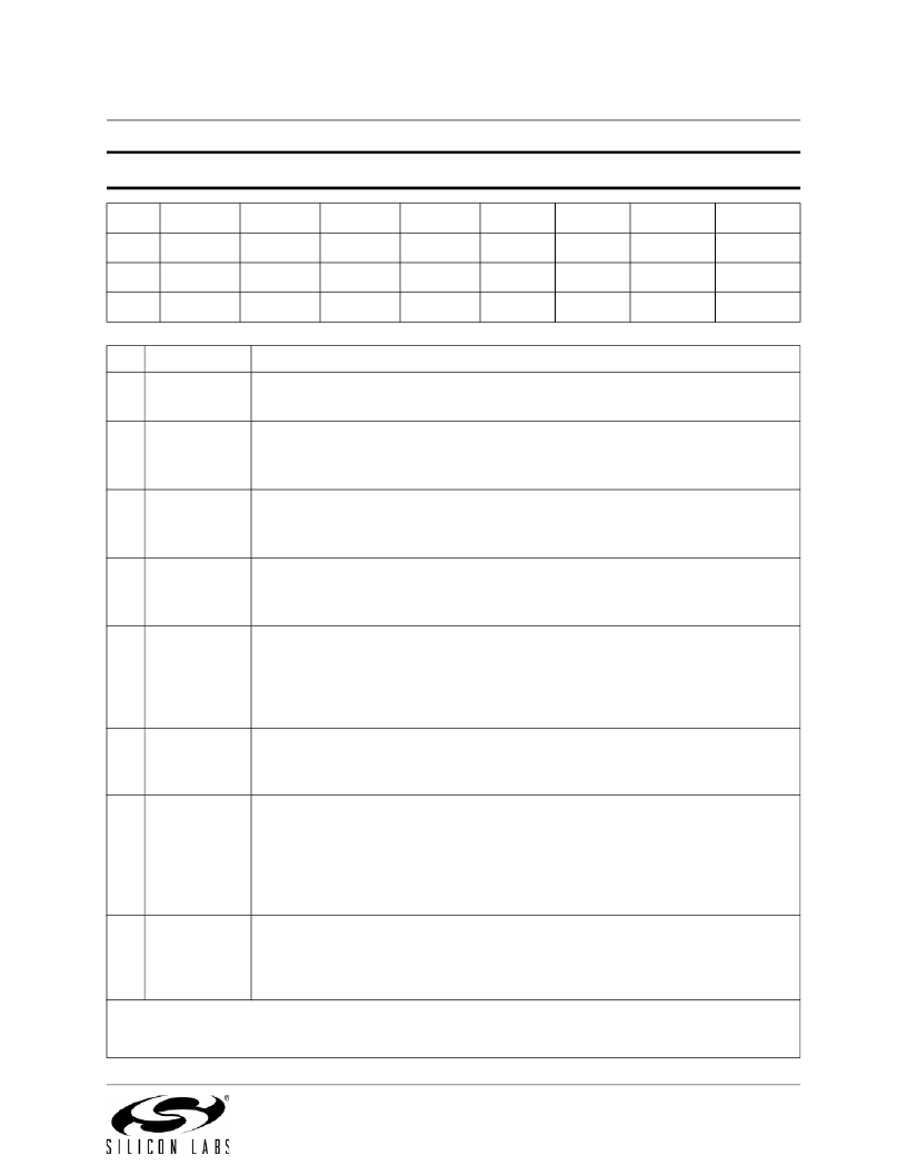
�SFR� Definition� 25.1.� SPI0CFG:� SPI0� Configuration�
�Bit�
�Name�
�Type�
�Reset�
�7�
�SPIBSY�
�R�
�0�
�6�
�MSTEN�
�R/W�
�0�
�5�
�CKPHA�
�R/W�
�0�
�4�
�CKPOL�
�R/W�
�0�
�3�
�SLVSEL�
�R�
�0�
�2�
�NSSIN�
�R�
�1�
�1�
�SRMT�
�R�
�1�
�0�
�RXBMT�
�R�
�1�
�SFR� Address� =� 0xA1;� SFR� Page� =� All� Pages�
�Bit� Name�
�Function�
�7�
�6�
�5�
�4�
�3�
�2�
�1�
�0�
�SPIBSY�
�MSTEN�
�CKPHA�
�CKPOL�
�SLVSEL�
�NSSIN�
�SRMT�
�RXBMT�
�SPI� Busy.�
�This� bit� is� set� to� logic� 1� when� a� SPI� transfer� is� in� progress� (master� or� slave� mode).�
�Master� Mode� Enable.�
�0:� Disable� master� mode.� Operate� in� slave� mode.�
�1:� Enable� master� mode.� Operate� as� a� master.�
�SPI0� Clock� Phase.�
�0:� Data� centered� on� first� edge� of� SCK� period.� *�
�1:� Data� centered� on� second� edge� of� SCK� period.� *�
�SPI0� Clock� Polarity.�
�0:� SCK� line� low� in� idle� state.�
�1:� SCK� line� high� in� idle� state.�
�Slave� Selected� Flag.�
�This� bit� is� set� to� logic� 1� whenever� the� NSS� pin� is� low� indicating� SPI0� is� the� selected�
�slave.� It� is� cleared� to� logic� 0� when� NSS� is� high� (slave� not� selected).� This� bit� does�
�not� indicate� the� instantaneous� value� at� the� NSS� pin,� but� rather� a� de-glitched� ver-�
�sion� of� the� pin� input.�
�NSS� Instantaneous� Pin� Input.�
�This� bit� mimics� the� instantaneous� value� that� is� present� on� the� NSS� port� pin� at� the�
�time� that� the� register� is� read.� This� input� is� not� de-glitched.�
�Shift� Register� Empty� (valid� in� slave� mode� only).�
�This� bit� will� be� set� to� logic� 1� when� all� data� has� been� transferred� in/out� of� the� shift�
�register,� and� there� is� no� new� information� available� to� read� from� the� transmit� buffer�
�or� write� to� the� receive� buffer.� It� returns� to� logic� 0� when� a� data� byte� is� transferred� to�
�the� shift� register� from� the� transmit� buffer� or� by� a� transition� on� SCK.� SRMT� =� 1� when�
�in� Master� Mode.�
�Receive� Buffer� Empty� (valid� in� slave� mode� only).�
�This� bit� will� be� set� to� logic� 1� when� the� receive� buffer� has� been� read� and� contains� no�
�new� information.� If� there� is� new� information� available� in� the� receive� buffer� that� has�
�not� been� read,� this� bit� will� return� to� logic� 0.� RXBMT� =� 1� when� in� Master� Mode.�
�Note:� In� slave� mode,� data� on� MOSI� is� sampled� in� the� center� of� each� data� bit.� In� master� mode,� data� on� MISO� is�
�sampled� one� SYSCLK� before� the� end� of� each� data� bit,� to� provide� maximum� settling� time� for� the� slave� device.�
�See� Table� 25.1� for� timing� parameters.�
�Rev.� 1.4�
�257�
�发布紧急采购,3分钟左右您将得到回复。
相关PDF资料
C8051F912DK
KIT DEV FOR C8051F91X/C8051F90X
C8051F930-TB
BOARD TARGET/PROTO W/C8051F930
C8051T610DB24
DAUGHTER BOARD T610 24QFN SOCKET
C8051T630DB20
BOARD SOCKET DAUGHTER 20-QFN
CAN-100
BOARD EVAL RS232 100QFP
CANADAPT28
KIT ADAPTER CANDEMOBOARD 28PLCC
CAT24AA01WI-GT3
IC EEPROM SERIAL 1KB I2C 8SOIC
CAT24AA02WI-G
IC EEPROM SERIAL 2KB I2C 8SOIC
相关代理商/技术参数
C8051F381
制造商:SILABS 制造商全称:SILABS 功能描述:USB DRIVER CUSTOMIZATION
C8051F381-GM
功能描述:8位微控制器 -MCU USB-64K-Flash
RoHS:否 制造商:Silicon Labs 核心:8051 处理器系列:C8051F39x 数据总线宽度:8 bit 最大时钟频率:50 MHz 程序存储器大小:16 KB 数据 RAM 大小:1 KB 片上 ADC:Yes 工作电源电压:1.8 V to 3.6 V 工作温度范围:- 40 C to + 105 C 封装 / 箱体:QFN-20 安装风格:SMD/SMT
C8051F381-GMR
功能描述:8位微控制器 -MCU USB-Flash-64k-ADC RoHS:否 制造商:Silicon Labs 核心:8051 处理器系列:C8051F39x 数据总线宽度:8 bit 最大时钟频率:50 MHz 程序存储器大小:16 KB 数据 RAM 大小:1 KB 片上 ADC:Yes 工作电源电压:1.8 V to 3.6 V 工作温度范围:- 40 C to + 105 C 封装 / 箱体:QFN-20 安装风格:SMD/SMT
C8051F381-GQ
功能描述:8位微控制器 -MCU USB-64K-Flash
RoHS:否 制造商:Silicon Labs 核心:8051 处理器系列:C8051F39x 数据总线宽度:8 bit 最大时钟频率:50 MHz 程序存储器大小:16 KB 数据 RAM 大小:1 KB 片上 ADC:Yes 工作电源电压:1.8 V to 3.6 V 工作温度范围:- 40 C to + 105 C 封装 / 箱体:QFN-20 安装风格:SMD/SMT
C8051F381-GQR
功能描述:8位微控制器 -MCU USB-Flash-64k-ADC RoHS:否 制造商:Silicon Labs 核心:8051 处理器系列:C8051F39x 数据总线宽度:8 bit 最大时钟频率:50 MHz 程序存储器大小:16 KB 数据 RAM 大小:1 KB 片上 ADC:Yes 工作电源电压:1.8 V to 3.6 V 工作温度范围:- 40 C to + 105 C 封装 / 箱体:QFN-20 安装风格:SMD/SMT
C8051F382
制造商:SILABS 制造商全称:SILABS 功能描述:USB DRIVER CUSTOMIZATION
C8051F382-GQ
功能描述:8位微控制器 -MCU USB-Flash-32k-ADC
RoHS:否 制造商:Silicon Labs 核心:8051 处理器系列:C8051F39x 数据总线宽度:8 bit 最大时钟频率:50 MHz 程序存储器大小:16 KB 数据 RAM 大小:1 KB 片上 ADC:Yes 工作电源电压:1.8 V to 3.6 V 工作温度范围:- 40 C to + 105 C 封装 / 箱体:QFN-20 安装风格:SMD/SMT
C8051F382-GQR
功能描述:8位微控制器 -MCU USB-Flash-32k-ADC RoHS:否 制造商:Silicon Labs 核心:8051 处理器系列:C8051F39x 数据总线宽度:8 bit 最大时钟频率:50 MHz 程序存储器大小:16 KB 数据 RAM 大小:1 KB 片上 ADC:Yes 工作电源电压:1.8 V to 3.6 V 工作温度范围:- 40 C to + 105 C 封装 / 箱体:QFN-20 安装风格:SMD/SMT